|
Part
the second. With explanatories. For those who is not
too abrupt, but wants to understand and understand.
The main moments - basic differences PPGA/FCPGA/FCPGA2.
The given chapter is intended already for those who
though understands a little, something was read on
the Internet, and as for those by whom too;) read
about impossibility / unreasonablenessly of realization
of the given remaking much and wants to find mistakes
in a material of given article (or, on the contrary,
articles about "impossibility";)
Besides, under the order: PPGA => FCPGA.
What has appeared essentially new in processors on
nucleus Coppermine from the point of view of "impossibility"
("danger") of job of the processors made
on new then 0.18-th technology? The equal bill - anything.
Added instructions SSE in any way do not prevent to
work to the processor in an old payment and demand
only small completion on the part of support the BIOS
(but it is solved software). The situation similar
to the same far-fetched transition in due time (Socket5->
Socket7) on processors with "MMX" a power
(is more correct - separate) by and large has repeated.
As well as then, main "argument" - the lowered
power of a nucleus. Actually, on it the long list
of "problems" came to an end. Therefore
all statements about " basic incompatibility
" sounding at that time under the relation of
processors on nucleus Coppermine to old motherboards
- pure water a marketing course. The main confirmation
of it is that fact, that the very first processors
Celeron Coppermine (566/600MHz, CPUID=683, Vcc=1.5V)
is completely safe (without remaking of a socket)
worked on PPGA motherboards (and thus were very not
bad overclocked).
However, to stop this "boundless situation";)
Intel has acted on "roughly" simply: for
that new processors did not work in old motherboards,
the signal of reset (RESET#, X4) "has been moved"
on place AH4 which in old motherboards earthed. In
result, at installation of the Coppermine-processor
in a PPGA-motherboard he don't started, always infinite
RESET. Plus to this leg AM2 became "key"
for FCPGA-processors in which she should be "
in air " - NotConnected/Reserved while in PPGA-motherboards
she " sits on the ground " (on ither too
have started "RESET#, is similar AH4).
Т.е., по большому счёту, для того, чтоб уговорить
работать Coppermine-процессор в старой плате нужно
всего лишь разобраться с "размножившимися"
"ресетами" - X4, мигрировавший в ножку AH4
(которую поэтому и надо соединить - "главным"
стал AH4, а в самом процессоре эти ноги не соединены)
плюс "обезвредить" совершенно не нужный
ресет AM2, подло "коротящий на землю" в
PPGA-платах.
Therefore the way of remaking is simple enough - we
isolate AM2 (usually unsolded contact from a socket)
and we throw the crosspiece between AH4 and X4.
As to a power then too all is simple enough. For
his installation legs VID0, VID1, VID2, VID3 and VID4
(last, generally, is marked as Vss-"ground"
that there was no opportunity to expose a voltage
above 2.05V, however, as a rule, in the majority of
PPGA-motherboards he on her "does not sit")
respond. Proceeding from a combination of signals
("0" - the ground or "1" - it
is not connected) on these legs{foots} the power unit
of the processor established on a motherboard exposes
the necessary voltage.
Table1. The combined table of voltage for
processors Slot1/Socket370.
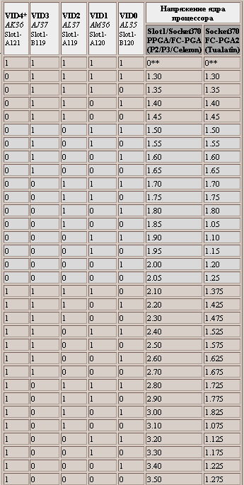
* - for FCPGA2 it VID25mV
** - in case of units on all "VID-ah" voltage
is not exposed in general (it is regarded as absence
of the processor) - 0 Volt.
First motherboards Slot1/PPGA (from submission Intel
that she will not make Slot1/Socket370-processors
with voltage Vcc less 1.8V) have been equipped Power
supply CPU, not supporting installation of processors
with a power is lower 1.8V (i.e. at installation of
the processor with smaller Vcc, the combination on
its legs VID0-VID4 was interpreted as 1/1/1/1/1, i.e.
in result it was exposed "0"). Therefore,
to bypass such problem it is necessary to establish
"compulsorily" Vcc> =1.8V. In case of
an opportunity of adjustment of a voltage (on an adapter
/ motherboard) it is necessary to expose simply the
necessary combination crosspieces (see table.1). If
such opportunity no, then it is necessary to make
it "manually". For example, if at you the
processor with a power 1.7V, means a configuration
of VID's - 0/0/1/1/1 then, having closed VID1 "
on the ground " (or even on the same, already
earthed in such processor, VID4 or VID3), we we shall
receive a combination 0/0/1/0/1 that corresponds 1.8V
which power supply CPU "knows" and will
correctly expose. Certainly, in that case the processor
will work on the overestimated voltage, however, first,
many (Vcc) all the same specially raise it ("
for overclocking "), and, second, (the greater
heating) always it is possible to overcome it with
the help simply a better cooler.
FCPGA => FCPGA2 (Tualatin).
If with Coppermine, basically, "non-believers";)
practically did not remain, with Tualatin all (I hope
- while;) it is more difficult. Processors with nucleus
Tualatin, under statements of numerous sources (it
is natural - first of all Intel), well, are exact
" are not compatible at all ":) with old
motherboards: and the power unit another is necessary
(VRM 8.5, instead of 8.4), and technology again more
"thin" - 0.13 instead of 0.18, and synchronization
there "new", and a power lower, and, at
last, the trunk has exchanged - AGTL instead of AGTL
+. We shall disassemble under the order.
AGTL.
"Main thing" - the "new" bus.
Already only absolute similarity of names casts some
doubts - like, the same, only without plus. Which,
probably, designated those 0.25V on which the level
of signals has gone down - in AGTL + he is equal 1.5V,
and in AGTL - 1.25V. Accordingly, from " official
documents " it turns out, that: "processors
Tualatin cannot correctly work on old parent motherboards
which give out a voltage on 20 % above necessary (as
the level of a voltage submitted on inputs of the
processor, should have disorder no more ±9%)".
And, really, if to address to "primary sources"
(the documentation on Taulatin from a site intel.com)
it is possible to read:
To item 4 it is in black and white written, what
yes, really, 1.25V +-9 % (and to develop - so, in
general, " with a sight " on +-3 %) and
it can't be helped. However somehow empty columns
Min and Max are suspiciously looked, and such "basic"
difference goes only as the note (and it read - only
the recommendation). Very much looks like the variant
"updated" by experts in marketing.
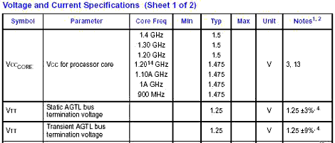
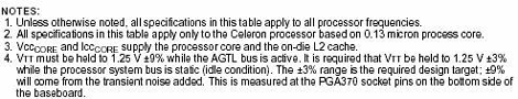
And, really, all clears up if to esteem page earlier:
Precisely and clearly (without any empty columns:),
a maximum - 1.75V. such " double standards ".:)
From here the first conclusion - Vtt=1.5V (i.e. the
level of signals, such as in old non Tualatin's motherboards)
for Tualatin is completely safe, as is essentially
below possible maximal value (and, means, it can be
overclocked and overclocked still:).
Differential synchronization.
Other "statement" - a "new" way
of the synchronization, "new" signal BCLK#
(inverted BCLK). In AGTL + "one" is used
for synchronization only BCLK (c by amplitude 2.5V),
and the "new" couple from opposite on polarity
BCLK/BCLK# (+1.25V and-1.25V) - so-called differential
synchronization here has appeared. As - for more stable
job such approach foggy speaks high frequencies. However
all in the same primary sources is in black and white
written:
I.e. the processor itself determines, what
way of synchronization to use proceeding from presence
of signal BCLK# on leg Y33. If he (BCLK#) there is
present, then the processor is switched in a mode
of differential synchronization, if no (and there
- only analog basic voltage +1.25V) it is switched
in "usual", old (single-ended) a mode with
"one" strobing pulse. Accordingly, the processor
inserted into system, "not knowing" differential
clocking, will simply be switched for a "usual"
way of synchronization (since supports both kinds).
Other signals (types / kinds) at AGTL the same, as
at AGTL + therefore on it the subject of the "new"
trunk can be closed.
VRM8.5
Concerning "more thin" technology, and,
accordingly, and lower voltage of a nucleus. In Tualutin,
for an opportunity to expose a voltage to within 0.025V
has been involved already becoming in PPGA/FCPGA unnecessary
VID4 (since he was used only at the task of a voltage
above 2.05V, and it already, naturally, has ceased
to be actual). At his installation (VID4) in "1"
to " standard (i.e. as at "old" PPGA/FCPGA-processors,
i.e. VRM8.4) it it is added 0.025V. Therefore this
signal (leg) and have named - "VID25mV"
(see table 1).
In case VID4 (VID25mV) it is equal "0" such
combination differs nothing from "old" (VRM8.4).
Accordingly, simply compulsorily having short-circuited
VID25mV " on the ground " (for that "old"
power supply CPU casually has not exposed proceeding
from unit on VID4 a huge voltage, so, for example,
at Tualatin with Vcc=1.475V, a combination = 1/1/1/0/0,
that corresponds 2.3V for "old" VRM8.4),
we shall safely solve this problem, i.e. we shall
receive a "correct" voltage with a rounding
off up to 0.5V in the smaller party. And at desire,
besides, with "accuracy" in 0.5V, always
it is possible to expose the necessary voltage "manually".
With new "VRM's" the couple of signals -
DYN_OE and VttPWRGD has appeared also. The first -
resolves installation VID0-4 and BSEL0-1 in the necessary
value, and the second is supervises.
The matter is that as against the previous processors
in Tualatin signals on VID's and BSEL's are not "analog"
(i.e. are simply set short-circuit inside their processor
" on the ground " - "0" or "
Not Connected " - "1"), and are exposed
by actually processor. I.e. initially they stay in
a status "NotConnected" (i.e. all "1"
- 0V). After reception "1" from leg DYN_OE
the processor exposes on them the necessary value
and supervises it on leg VttPWRGD - if there too "1"
(and her and should form VRM8.5), all Ok.
"As always";), both these legs (AN3 - DYN_OE
and AK4 - VttPWRGD) in PPGA/FCPGA are "grounds".
Therefore both of them need to be isolated at remaking.
Plus difficulty consists that on AK4 (VttPWRGD) except
for isolation from the ground is necessary to submit
"1" (Vtt) since differently astable unit
(more precisely, there at all unit, and " infinite
resistance " there turns out), that is especially
shown at sharp increase of loading on the processor.
It as it was spoken above, will make some (more precisely
- the most important)difficulty at remaking "
under Tualatin", however it is necessary
for stable job.
In the end - about a popular belief - "basic"
difference VRM8.5 which "is able" to lower
a power with growth of a current of consumption. This
ridiculous conclusion has been made from appeared
in the documentation on VRM8.5 tables:
Actually, certainly, all is banal - the schedule
represents only "standardization" of that
as so always is present at any power supply - decrease
in a target voltage at increase of a current of loading.
Speaking is exaggerated, he demands, that the target
voltage changed no more, than on ~0.15V in all a range
of change of a current of consumption of the processor
(in 8.4 were precisely same "frameworks",
exact values on all range of change of a current only
have not been painted).
RESET2#.
Well, and at the end, besides, "as always":,
signal RESET# "was multiplied" - he has
appeared on, next and, certainly:, a "earthed"
leg - AJ3. Here any differences from Coppermine a
case, a way of "treatment" - simply to isolate
(AJ3).
Part 1. Part
3. Part 4.
|